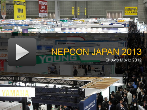
NEPCON JAPAN 2012於今年元月18~20日三天在東京有明國際展覽中心舉行,該展會始於1972年為致力提升日本電子產業發展而創辦,30多年來,隨著日本電子產業發展,舉辦規模逐年擴大,現今已成為全球知名的電子封裝國際指標展覽會。2000年起,NEPCON JAPAN為充實展出內容,參展範圍除了既有的生產設備外,更增加了如IC封裝技術、PCB、電子元件以及先進材料等相關產品及技術。同屬此展會還包含41st國際電子製造安裝展、13th半導體IC封裝技術展、13th印刷電路板展等三大展覽。
由於展覽規模與主題相當包羅萬象,各大展覽項下另含括主辦單位每年為新趨勢所開辦的展會,包含INTERNEPCON JAPAN展主要是彙聚各種電子產品製造和SMT所用設備與材料技術、ELECTROTEST JAPAN為日本最大的專注於電子製造和研發檢測技術的展覽會、IC PACKAGING TECHNOLOGY EXPO則專注於傳感器、MEMS器材和光器材所需IC終端製造及封裝技術、ELE EXPO–ELECTRONIC COMPONENTS EXPO為展出日本最有影響力的家電,工業用,通信行業所需各種電子元件、PWB EXPO–Printed Wiring Boards Expo特別展出各種印刷電路板、模板、設計服務及CAD工具、MATERIAL JAPAN–Advanced Electronic Materials Expo專注電子材料和技術的商務展會、MicroTech JAPAN–Micro Fabrication /Fine Process Technology Expo專注各種電子製造業加工技術展覽會。
今年41st NEPCON JAPAN×ELECTRONIX R&D JAPAN展為亞洲最大規模電子技術展會,此展會共匯集1,217家參展廠商以及59,963位參訪者。由於智慧型手機越來越強調輕薄且高功能之重要性時,相對在今年的技術研發方向也將更關注高密度封裝技術及測試技術的可靠度。今年參展大廠除了OMRON、 NAGOYA ELECTRIC WORKS、Saki Corporation外,還新加入如SANKO TSUSHO、TOYOTSU MACHINERY現場展示最新的測試設備,工業領導廠商KUSUMOTO Chemicals也展示能符合多種條件操作下的尖端測試設備。今年展場中,電力電子展區的規模正逐漸擴大,包括Nippon Kayaku展示在高電流下的散熱樹脂、KYOTO DENKI, AVERY DENNISON JAPAN MATERIALS, NAGASE INTEGREX等廠商也聚焦於電力電子領域,預計此領域具未來成長的潛力。在專門技術研討會的部分,主辦單位根據今年特別邀請135位專家共舉辦48場研討會,從各場研討會的主講者與主題中,可瞭解目前國際大廠所發展的技術與市場動態。
在13th IC PACKAGING TECHNOLOGY EXPO半導體構裝主題中,例如Sumitomo Bakelite、NAMICS、Hitachi Chemical三大廠共同發表最新的IC封裝材料技術。BOSCH、DENSO、Renesas Electronics共同提出未來汽車電子與IC封裝技術。對於最近流行的智慧型手機、平板、Ultra-books的先進封裝技術也受到關注,由Toshilba、J-Devices、Stats ChipPac Korea做共同的討論與發表。另外,半導體製造趨勢、LED封裝技術與密封材現況、MEMS技術的實際應用與技術挑戰、3D 封裝的創新、銅焊線製程等主題也有所著墨。
41th INTERNEPCON JAPAN |
Development of Pb-free Soldering Options and Reliability |
Current Market and Technical Trends of Touch Panels with Rapidly-growing Applications |
Industry Leaders' View: Strength of "Japan's Manufacturing Technologies" |
Latest Trends of Micro-bump and Interconnection Technologies |
Perspectives and Challenges of Automotive Electronic Mounting |
High-quality Production System in Mounting Process and Recent Updates on Advanced Testing & Analysis Technology |
Forefront of Power Device Mounting and Heat Radiation Technologies |
Leading-edge Technology for Further-evolving Printed Electronics |
Striking Progress of Smart Phone Mounting Technology |
Nanoparticle Manufacturing and Fine-pitch Mounting Technologies |
LED Device Mounting Technology and its Development Trends |
13th IC PACKAGING TECHNOLOGY EXPO |
IC Packaging Roadmaps for Smaller and Thinner Package with Higher Function |
Latest Material Technology for Advanced IC Packaging |
Latest Trends of Semiconductor Manufacturers Worldwide |
Recent Status of LED Mounting Technology and Sealing Materials |
Future Outlook of Semiconductor Business -Keys to Enhance Electronics Industry |
Future Outlook of Semiconductor Business -Keys to Enhance Electronics Industry |
Smartphones, Tablets & Ultra-books─Most-advanced Packaging Technology |
Cutting Edge of MEMS Technology ─Practical Applications and Technical Challenges |
Lecture by Leading Authority in Automotive Semiconductor Packaging Field |
Evolving 3D Packaging Innovates Devices and the World |
Future of Automotive Electronics & IC Packaging Technology |
Current Industry Trend in China |
Lecture by Taiwan's No.1 LED Manufacturer |
Most-current Development Trends in Power Devices for Power Saving |
Keys to Cost Reduction─Recent Copper Wirebonding Technology |
PWB EXPO |
High-thermal Conductivity Resin Substrates with Growing Attention from Automotive and Smartphone Applications |
Latest FPC Market and Technology Trends |
Latest Technology Trends in LED Heat Radiation Design and Materials |
Ultrafine Processing Technology at the Forefront |
Front-line Technology of Further Developing Printed Electronics |
Technical Solutions to Achieve Thinner Mobile Devices |
Top Manufacturers Reveal their Strategies and Future Visions |
Advanced PCB Materials Pioneer the Future—Cutting-edge Technology Development |
Next-generation PCB and Interposer—Possibility of LSI Global Interconnects |
New Technology and Materials for Buildup PCB for Smartphones and Tablets |
Universal Prevalence of Built-in Technology—Industry Trends and Simulation & Component Technology |
本文圖片及影片來源:Reed Exhibitions Japan Ltd
作者:材料世界網 編輯室